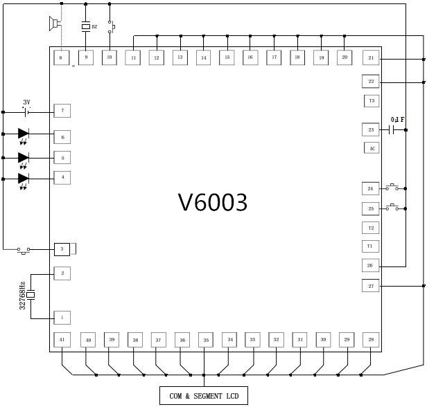
V6003
6 Digit LCD Alarm Watch with Alarm/Chronograph
FUNCTIONS
* Split operative stopwatch (Accurate to 1/100 second)
* Hour,Minute,Second,Month and Day normal display
* 6 digit chronograph: Auto ranging after 30 minutes tohour,minute,second,from minute,second,1/100 second
* Alarm output for melody IC
* Alarm function with 4 to 5 minutes snooze
* Use selectable 12/24 format & 4 year calendar
* Chime on every hour
* One touch correction of time error within ±30 seconds
* Oscillating build-in capacitor
* Direct drive of piezo buzzer
* Pad ALAB is build-in transister
* RGB Backlight control output
Characteristics | Sym | Min | Typ | Max | Unit | REMARKS |
Ope rating Voltag e | Vdd | 3.0 | V | - | ||
Q uie s c e nt C urre nt | Idd1 | - | 0.9 | 1.2 | µA | No Load |
O pe rati ng C urre nt | Idd2 | - | 6- | 9 | mA | RGB |
Input high voltage | Vih | Vdd-0.3 | - | Vdd | V | - |
Input low voltage | Vil | Vss | - | Vss+0.3 | V | - |
Switch activation current | Isw | - | - | 4 | µA | Vin=Vdd |
Oscillating start voltage | Vosc | - | - | 1.2 | V | Within 3 seconds |
Alarm drive current | Iol | 5 | 10 | - | mA | Vala=0.5V pad=7 |
O s c illa ting inp ut F re q ue nc y | Fosc | - | 32768 | - | Hz | ±30%Tol |
L CD f re que nc y | Flcd | - | 32 | - | Hz | - |
Time stability | Tstb | - | 1 | - | ppm | - |
Output curre nt for IND, DIS | Io | 1 | - | mA | Vo=0.5V |
Pad | Name | Pad | Name | Pad | Name | Pad | Name |
1 | OSCI | 12 | PM/AM | 23 | VSS | 34 | G4/D4 |
2 | OSCO | 13 | A1/SUN | 24 | D | 35 | F4/E4 |
3 | L | 14 | C1/B1 | 25 | S | 36 | B3/C3 |
4 | RL | 15 | A2/MON | 26 | VDD | 37 | G3/D3 |
5 | GL | 16 | CL/TUE | 27 | B6/C6 | 38 | F3/E3 |
6 | BL | 17 | A3/WED | 28 | G6/D6 | 39 | B2/C2 |
7 | GND | 18 | A4/THU | 29 | F6/E6 | 40 | G2/D2 |
8 | ALAB | 19 | A5/FRI | 30 | B5/C5 | 41 | F2/E2 |
9 | ALA1 | 20 | A6/SAT | 31 | G5/D5 | ||
10 | M | 21 | DTE/AL | 32 | F5/E5 | ||
11 | COM2 | 22 | COM1 | 33 | B4/C4 |

Note:
1. L = 1.8 ~ 2.0 mH / 17 ~ 12 Ω,
according to the light emitting chip capacitor value and choice, R = 10 k Ω;
2. C1=0.1 F;
3. The PAD propagated and ALA1 feet as the rings at the output, the application either;
4. Pick VDD substrate;
5. The T1, T2, T3, and AC test.
QQ: 10298183192
手机:18312529938
电话: 0755-28796192
邮箱: 10298183192@qq.com
地址:Liulian Xuekeng Industry Zone,Pingdi Town,Longgang Area,Shenzhen City